- 您现在的位置:买卖IC网 > Sheet目录345 > MT42L256M32D4KP-3 IT:A (Micron Technology Inc)IC LPDDR2 SDRAM 8GBIT 168FBGA
�� �
�
�2Gb:� x16,� x32� Mobile� LPDDR2� SDRAM� S4�
�Electrical� Specifications�
�Electrical� Specifications�
�Absolute� Maximum� Ratings�
�Stresses� greater� than� those� listed� below� may� cause� permanent� damage� to� the� device.�
�This� is� a� stress� rating� only,� and� functional� operation� of� the� device� at� these� or� any� other�
�conditions� outside� those� indicated� in� the� operational� sections� of� this� document� is� not�
�implied.� Exposure� to� absolute� maximum� rating� conditions� for� extended� periods� may�
�adversely� affect� reliability.�
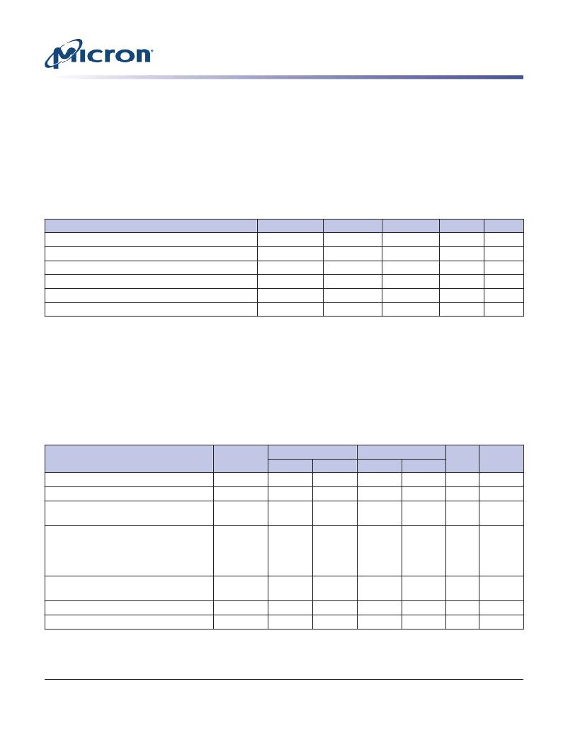
�Table� 54:� Absolute� Maximum� DC� Ratings�
�Parameter�
�V� DD1� supply� voltage� relative� to� V� SS�
�V� DD2� supply� voltage� relative� to� V� SS�
�V� DDCA� supply� voltage� relative� to� V� SSCA�
�V� DDQ� supply� voltage� relative� to� V� SSQ�
�Voltage� on� any� ball� relative� to� V� SS�
�Storage� temperature�
�Symbol�
�V� DD1�
�V� DD2� (1.2V)�
�V� DDCA�
�V� DDQ�
�V� IN� ,� V� OUT�
�T� STG�
�Min�
�–0.4�
�–0.4�
�–0.4�
�–0.4�
�–0.4�
�–55�
�Max�
�+2.3�
�+1.6�
�+1.6�
�+1.6�
�+1.6�
�+125�
�Unit�
�V�
�V�
�V�
�V�
�V�
�?C�
�Notes�
�1�
�1�
�1,� 2�
�1,� 3�
�4�
�Notes:�
�1.�
�2.�
�3.�
�4.�
�See� 1.� Voltage� Ramp� under� Power-Up� (page� 40).�
�V� REFCA� 0.6� ≤� V� DDCA� ;� however,� V� REFCA� may� be� ≥� V� DDCA� provided� that� V� REFCA� ≤� 300mV.�
�V� REFDQ� 0.6� ≤� V� DDQ� ;� however,� V� REFDQ� may� be� ≥� V� DDQ� provided� that� V� REFDQ� ≤� 300mV.�
�Storage� temperature� is� the� case� surface� temperature� on� the� center/top� side� of� the� de-�
�vice.� For� measurement� conditions,� refer� to� the� JESD51-2� standard.�
�Input/Output� Capacitance�
�Table� 55:� Input/Output� Capacitance�
�Note� 1� applies� to� all� parameters� and� conditions�
�LPDDR2� 1066-466�
�LPDDR2� 400-200�
�Parameter�
�Input� capacitance,� CK� and� CK#�
�Input� capacitance� delta,� CK� and� CK#�
�Input� capacitance,� all� other� input-�
�Symbol�
�C� CK�
�C� DCK�
�C� I�
�MIN�
�1.0�
�0�
�1.0�
�MAX�
�2.0�
�0.20�
�2.0�
�MIN�
�1.0�
�0�
�1.0�
�MAX�
�2.0�
�0.25�
�2.0�
�Unit�
�pF�
�pF�
�pF�
�Notes�
�2,� 3�
�2,� 3,� 4�
�2,� 3,� 5�
�only� pins�
�Input� capacitance� delta,� all� other� input-�
�C� DI�
�–0.40�
�+0.40�
�–0.50�
�+0.50�
�pF�
�2,� 3,� 6�
�only� pins�
�Input/output� capacitance,� DQ,� DM,� DQS,�
�C� IO�
�1.25�
�2.5�
�1.25�
�2.5�
�pF�
�2,� 3,� 7,� 8�
�DQS#�
�Input/output� capacitance� delta,� DQS,�
�C� DDQS�
�0�
�0.25�
�0�
�0.30�
�pF�
�2,� 3,� 8,� 9�
�DQS#�
�Input/output� capacitance� delta,� DQ,� DM�
�Input/output� capacitance� ZQ�
�C� DIO�
�C� ZQ�
�–0.5�
�0�
�+0.5�
�2.5�
�–0.6�
�0�
�+0.6�
�2.5�
�pF�
�pF�
�2,� 3,� 8,� 10�
�2,� 3,� 11�
�Notes:�
�1.� T� C� –25?C� to� +105?C;� V� DDQ� =� 1.14–1.3V;� V� DDCA� =� 1.14–1.3V;� V� DD1� =� 1.7–1.95V;� V� DD2� =� 1.14–�
�1.3V.�
�PDF:� 09005aef83f3f2eb�
�2gb_mobile_lpddr2_s4_g69a.pdf� –� Rev.� N� 3/12� EN�
�113�
�Micron� Technology,� Inc.� reserves� the� right� to� change� products� or� specifications� without� notice.�
�2010� Micron� Technology,� Inc.� All� rights� reserved.�
�发布紧急采购,3分钟左右您将得到回复。
相关PDF资料
MT45W1MW16BDGB-708 AT
IC PSRAM 16MBIT 104MHZ 54VFBGA
MT48H32M16LFB4-75B IT:C
IC SDRAM 512MB 54VFBGA
MT48H8M16LFB4-75 IT:K TR
IC SDRAM 128MBIT 133MHZ 54VFBGA
MTC100-JA2-P34
CONTACT INSERT PIN
MX841BE
IC CONVERTER WHITE LED 8-SOIC
MXHV9910BTR
IC LED DRIVER HIGH BRIGHT 8-SOIC
MXN12FB12F
MOTOR BRUSHED DC 12V 2922RPM
MXN13FB08B1
MOTOR BRUSHED DC 8V 4714RPM
相关代理商/技术参数
MT42L256M32D4KP-MS
制造商:Micron Technology Inc 功能描述:256MX32 LPDDR2 PLASTIC IND TEMP GREEN WFBGA 1.2V - Bulk